Glass components for semiconductor manufacturing
Heat, plasma and chemistry: in semiconductor manufacturing, glass components must deliver process stability without contamination. MDI processes carrier, cover and equipment glass — for semiconductor manufacturing equipment and wafer processing, from 30 µm, from prototype to series.
Send us your specification →What we supply for semiconductor manufacturing
Glass components across the semiconductor value chain — from ultra-thin glass carriers to precision parts for fab equipment, with traceability built in.
Ultra-thin glass
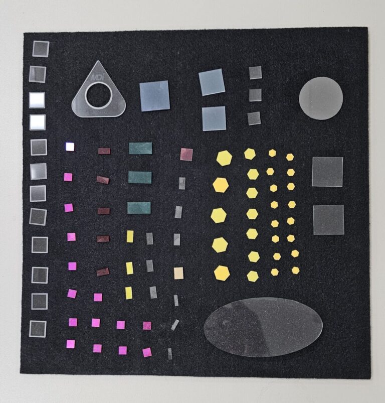
Laser cutting from 30 µm (CO2); SOLID-D® cutting tools for glass up to 100 µm — carriers, cover glasses, spacers. Fast-growing market context: high-index glass wafers for AR waveguide manufacturing.
Traceability
In-glass data matrix marking with 20 µm feature size.
Coating removal & patterning
Selective, layer-accurate ablation on coated glass.
Components for fab equipment
Laser drilling from Ø 1 mm, stepped holes and inside contours.
Glass is moving into the package
Advanced semiconductor packaging is shifting towards glass: glass core substrates, panel-level packaging (PLP), carrier wafers for heterogeneous integration and co-packaged optics — driven by AI and high-performance computing chips. Leading chip and substrate makers are investing in glass-core technology. This transition makes precision glass processing the decisive link: singulation, edge quality, splinter-free cutting of thin panels, and the handling components around the process.
Part of the value chain. The next package generation is built in collaboration across the semiconductor value chain — material makers, substrate developers and processing partners. MDI is the processing link: singulation, edge processing, prototypes and small series. The collaboration starts before the first series specification — send us yours.
Process window
Which process applies
Links to the existing process pages — URLs unchanged.

Precision components for fab equipment
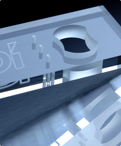
Material: glass, t = 4 mm. Geometry: inside contour 58 × 58 mm, stepped holes and laser-drilled holes from Ø 1 mm. Result: contactless processing without micro-cracks — example geometry from the MDI application portfolio.
Can you process fused quartz / fused silica components?
Suitability depends on the material and the geometry of the part. Send us your specification — we will assess it and get back to you.
Do you process glass core substrates or panel-level packaging formats?
That depends on format, thickness and process step. Send us your specification — we will assess feasibility case by case.
Glass components from prototype to series
Carriers, covers and equipment parts on MDI’s own laser and cutting-wheel systems — low volumes, frequent iteration, no capital commitment. Send a drawing and we handle the rest.
Send us your specification →